

For non-destructive optical characterization, laser beam induced current (LBIC) microscopy has been developed into as a quantitative tool to examine individual photodiodes within a large pixel array. Two-dimensional LBIC microscopy, also generally called photocurrent mapping (PC mapping), can provide spatially resolved information about local electrical properties and p-n junction formation in photovoltaic infrared (including visible light) photodetectors from which it is possible to extract material and device parameters such as junction area, junction depth, diffusion length, leakage current position and minority carrier diffusion length etc. This paper presents a comprehensive review of research background, operating principle, fundamental issues, and applications of LBIC or PC mapping.
State Key Program for Basic Research of China(2014CB921600)
National Natural Science Foundation of China(11322441)
Fund of Shanghai Science and Technology Foundation(14JC1406400)
[1] Wallmark J T. A new semiconductor photocell using lateral photoeffect. Proc IRE, 1956, 45: 474-483 Google Scholar
[2] Bajaj J, Bubulac L O, Newman P R, et al. Spatial mapping of electrically active defects in HgCdTe using laser beam induced current. J Vac Sci Technol A, 1987, 5: 3186-3187 CrossRef Google Scholar
[3] Musca C A, Redfern D A, Dell J M, et al. Laser beam induced current as a tool for HgCdTe photodiode characterization. Microelectron J, 2000, 31: 537-544 CrossRef Google Scholar
[4] Redfern D A, Smith E, Musca C A, et al. Interpretation of current flow in photodiode structures using laser beam-induced current for characterization and diagnostics. IEEE Trans Electron Dev, 2006, 53: 23-31 CrossRef Google Scholar
[5] Hu W D, Chen X S, Ye Z H, et al. Polarity inversion and coupling of laser beam induced current in As-doped long-wavelength HgCdTe infrared detector pixel arrays: Experiment and simulation. Appl Phys Lett, 2012, 101: 181108 CrossRef Google Scholar
[6] Hu W D, Chen X S, Ye Z H, et al. Dependence of ion-implant- induced LBIC novel characteristic on excitation intensity for long- wavelength HgCdTe-based photovoltaic infrared detector pixel arrays. IEEE J Sel Top Quant, 2013, 19: 4100107 Google Scholar
[7] Feng A L, Li G, He G, et al. The role of localized junction leakage in the temperature-dependent laser-beam-induced current spectra for HgCdTe infrared focal plane array photodiodes. J Appl Phys, 2013, 114: 173107 CrossRef Google Scholar
[8] Redfern D A, Musca C A, Dell J M, et al. Correlation of laser-beam- induced current with current-voltage measurements in HgCdTe photodiodes. J Electron Mater, 2004, 33: 560-571 CrossRef Google Scholar
[9] Redfern D A, Musca C A, Dell J M, et al. Characterization of electrically active defects in photovoltaic detector arrays using laser beam- induced current. IEEE Trans Electron Dev, 2005, 52: 2163-2174 CrossRef Google Scholar
[10] Yin F, Hu W D, Zhang B, et al. Simulation of laser beam induced current for HgCdTe photodiodes with leakage current. Opt Quantum Electron, 2009, 41: 805-810 CrossRef Google Scholar
[11] Redfern D A, Thomas J A, Musca C A, et al. Diffusion length measurements in p-HgCdTe using laser beam induced current. J Electron Mater, 2001, 30: 696-703 CrossRef Google Scholar
[12] Musca C A, Redfern D A, Smith E, et al. Junction depth measurement in HgCdTe using laser beam induced current (LBIC). J Electron Mater, 1999, 28: 603-610 CrossRef Google Scholar
[13] Gluszak E A, Hinckley S, Kamran E. Determination of junction depth and related current phenomena using laser-beam-induced current. Proc SPIE, 2004, 5274: 331-341 CrossRef Google Scholar
[14] Hu W D, Chen X S, Yin F, et al. Analysis of temperature dependence of dark current mechanisms for long-wavelength HgCdTe photovoltaic infrared detectors. J Appl Phys, 2009, 105: 104502 CrossRef Google Scholar
[15] Hu W D, Chen X S, Ye Z H, et al. Accurate simulation of temperature dependence of dark current in HgCdTe infrared detector assisted by analytical modeling. J Electron Mater, 2010, 39: 981-985 CrossRef Google Scholar
[16] Zha F X, Zhou S M, Ma H L, et al. Laser drilling induced electrical type inversion in vacancy-doped p-type HgCdTe. Appl Phys Lett, 2008, 93: 151113 CrossRef Google Scholar
[17] Zha F X, Li M S, Shao J, et al. Femtosecond laser-drilling-induced HgCdTe photodiodes. Opt Lett, 2010, 35: 971-973 CrossRef Google Scholar
[18] Zhou S M, Zha F X, Guo Q T, et al. The morphology of micro hole pn junction in p-type HgCdTe formed by femtosecond laser drilling. J Infrared Millim Waves, 2010, 29: 337-341 Google Scholar
[19] Martyniuk M, Sewell R H, Westerhout R, et al. Electrical type conversion of p-type HgCdTe induced by nanoimprinting. Appl Phys, 2011, 109: 096102 CrossRef Google Scholar
[20] Gluszak E A, Hinckley S. Contactless junction contrast of HgCdTe n-on-p-type structures obtained by reactive ion etching induced p-to-n conversion. J Electron Mater, 2001, 30: 768-773 CrossRef Google Scholar
[21] Fang W, Ito K, Redfern D A. Parameter identification for semiconductor diodes by LBIC imaging. SIAM J Appl Math, 2002, 62: 2149-2174 CrossRef Google Scholar
[22] Hong X K, Lu H, Zhang D B. Study on the structure characteristics of HgCdTe photodiodes using laser beam-induced current. Opt Quantum Electron, 2013, 45: 623-628 CrossRef Google Scholar
[23] Bajaj J, Tennant W E, Newman P R. Laser beam induced current imaging of surface nonuniformity at the HgCdTe/ZnS interface. J Vac Sci Technol A Vac Surf Films, 1988, 6: 2757-2759 CrossRef Google Scholar
[24] Bajaj J, Tennant W E, Zucca R, et al. Spatially resolved characterization of HgCdTe materials and devices by scanning laser microscopy. Semicond Sci Technol, 1993, 8: 872-887 CrossRef Google Scholar
[25] Redfern D A, Fang W, Ito K, et al. Low temperature saturation of p-n junction laser beam induced current signals. Solid-State Electron, 2004, 48: 409-414 CrossRef Google Scholar
[26] Qiu W C, Cheng X A, Wang R, et al. Novel signal inversion of laser beam induced current for femtosecond-laser-drilling induced junction on vacancy-doped p-type HgCdTe. J Appl Phys, 2014, 115: 204506 CrossRef Google Scholar
[27] Busenberg S, Fang W, Ito K. Modeling and analysis of laser beam induced current images in semiconductors. SIAM J Appl Math, 1993, 53: 187-204 CrossRef Google Scholar
[28] Qiu W C, Hu W D, Lin T, et al. Temperature-sensitive junction transformations for mid-wavelength HgCdTe photovoltaic infrared detector arrays by laser beam induced current microscope. Appl Phys Lett, 2014, in press. Google Scholar
[29] Hu W D, Ye Z H, Liao L, et al. A 128×128 long-wavelength/mid- wavelength two-color HgCdTe infrared focal plane array detector with ultra-low spectral crosstalk. Opt Lett, 2014, 39: 5130-5133 CrossRef Google Scholar
[30] Feng A L, Li G, He G, et al. Dependence of laser beam induced current on geometrical sizes of the junction for HgCdTe photodiodes. Opt Quantum Electron, 2014, 46: 1277-1282 CrossRef Google Scholar
[31] Baugher B, Churchill H, Yang Y F, et al. Optoelectronic devices based on electrically tunable p-n diodes in a monolayer dichalcogenide. Nat Nanotech, 2014, 9: 262-267 CrossRef Google Scholar
[32] Balasubramanian K, Burghard M, Kern K, et al. Photocurrent imaging of charge transport barriers in carbon nanotube devices. Nano Lett, 2005, 5: 507-510 CrossRef Google Scholar
[33]
Zhang
Y P,
Deng
W,
Zhang
X J, et al.
[34] Buscema M, Groenendijk D J, Steele G A, et al. Photovoltaic effect in few-layer black phosphorus PN junctions defined by local electrostatic gating. Nature Commun, 2014, 5: 4651 CrossRef Google Scholar
[35] Yu Y Q, Jie J S, Jiang P, et al. High-gain visible-blind UV photodetectors based on chlorine-doped n-type ZnS nanoribbons with tunable optoelectronic properties. J Mater Chem, 2011, 21: 12632-12638 CrossRef Google Scholar
[36] Wang J L, Zou X M, Xiao X H, et al. Floating gate memory based monolayer MoS2 transistor with metal nanocrystals embedded in gate dielectrics. Small, 2014, doi: 10.1002/smll.201401872. Google Scholar
[37] Hu W D, Chen X S, Yin F, et al. Simulation and design consideration of photoresponse for HgCdTe infrared photodiodes. Opt Quantum Electron, 2008, 40: 1255-1260 CrossRef Google Scholar
[38] Guo N, Hu W D, Chen X S, et al. Optimization for mid-wavelength InSb infrared focal plane arrays under front-side illumination. Opt Quantum Electron, 2013, 45: 673-679 CrossRef Google Scholar
[39] Hu W D, Chen X S, Ye Z H, et al. An improvement on short wavelength photoresponse for a heterostructure HgCdTe two-color infrared detector. Semicond Sci Technol, 2010, 25: 045028 CrossRef Google Scholar
[40] Wenus J, Rutkowski J, Rogalski A. 2D analysis of double layer heterojunction HgCdTe photodiodes. IEEE Trans Electron Devices, 2001, 48: 1326-1332 CrossRef Google Scholar
[41] Orsogna D D, Tobin S, Bellotti E. Numerical analysis of a very long-wavelength HgCdTe pixel array for infrared detection. J Electron Mater, 2008, 37: 1349-1355 CrossRef Google Scholar
[42] Keasler C A, Moresco M, Orsogna D D, et al. 3D numerical analysis of As-diffused HgCdTe planar pixel arrays. Proc SPIE, 2010, 7780: 77800J CrossRef Google Scholar
[43]
Ji
X L,
Liu
B Q,
Xu
Y, et al.
Deep-level traps induced dark currents in extended wavelength In
[44] Yin F, Hu W D, Quan Z J, et al. Determination of electron diffusion length in HgCdTe photodiodes using laser beam induced current. Acta Phys Sin, 2009, 58: 7885-7889 Google Scholar
[45] Ong V, Wu D. Determination of diffusion length from within a confined region with the use of EBIC. IEEE Trans Electron Dev, 2001, 48: 332-337 CrossRef Google Scholar
[46] Bubulac L O, Tennant W E. Role of Hg in junction formation in ion-implanted HgCdTe. Appl Phys Lett, 1987, 51: 355-357 CrossRef Google Scholar
[47] Bubulac L O. Dependence of junction formation on substrate in implanted HgCdTe. Appl Phys Lett, 1985, 46: 976-978 CrossRef Google Scholar
[48] Arias J M, Zandian M, Bajaj J, et al. Molecular beam epitaxy HgCdTe growth-induced void defects and their effect on infrared photodiodes. J Electron Mater, 1995, 24: 521-524 CrossRef Google Scholar
[49] Buell A A, Pham L T, Newton M D, et al. Physical structure of molecularbeam epitaxy growth defects in HgCdTe and their impact on two-color detector performance. J Electron Mater, 2004, 33: 662-666 CrossRef Google Scholar
[50] Ahn Y H, Tsen A W, Kim B, et al. Photocurrent Imaging of p-n Junctions in Ambipolar Carbon Nanotube Transistors. Nano Lett, 2007, 7: 3320-3323 CrossRef Google Scholar
[51] Balasubramanian K, Fan Y W, Burghard M, et al. Photoelectronic transport imaging of individual semiconducting carbon nanotubes. Appl Phys Lett, 2004, 84: 2400-2402 CrossRef Google Scholar
[52] Freitag M, Tsang J C, Bol A, et al. Imaging of the schottky barriers and charge depletion in carbon nanotube transistors. Nano Lett, 2007, 7: 2037-2042 CrossRef Google Scholar
[53] Xia F N, Mueller T, Golizadeh-mojarad R, et al. Photocurrent imaging and efficient photon detection in a graphene transistor. Nano Lett, 2009, 9: 1039-1044 CrossRef Google Scholar
[54] Wu C C, Jariwala D, Sangwan V K, et al. Elucidating the photoresponse of ultrathin MoS2 field-effect transistors by scanning photocurrent microscopy. J Phys Chem Lett, 2013, 4: 2508-2513 CrossRef Google Scholar
[55] Oriol L S, Dominik L, Metin K, et al. Ultrasensitive photodetectors based on monolayer MoS2. Nat Nanotech, 2013, 8: 497-501 CrossRef Google Scholar
[56] Britnell L, Ribeiro R M, Eckmann A, et al. Strong light-matter interactions in heterostructures of atomically thin films. Science, 2013, 340: 1311-1314 CrossRef Google Scholar
[57] Song X F, Hu J L, Zeng H B. Two-dimensional semiconductors: Recent progress and future perspectives. J Mater Chem C, 2013, 1: 2952-2969 CrossRef Google Scholar
[58] Zeng H B, Zhi C Y, Zhang Z H, et al. “White” graphene: Boron nitride nanoribbons via boron nitride nanotube unwrapping. Nano Lett, 2010, 10: 5049-5055 CrossRef Google Scholar
[59] Ahn Y, Dunning J, Park J. Scanning photocurrent imaging and electronic band studies in silicon nanowire field effect transistors. Nano Lett, 2005, 5: 1367-1370 CrossRef Google Scholar
[60] Gu Y, Kwak E, Lensch J, et al. Near-field scanning photocurrent microscopy of a nanowire photodetector. Appl Phys Lett, 2005, 87: 043111 CrossRef Google Scholar
[61] Miao J S, Hu W D, Guo N, et al. Single InAs nanowire room- temperature near-infrared photodetectors. ACS Nano, 2014, 8: 3628-3635 CrossRef Google Scholar
[62] Dufaux T, Boettcher J, Burghard M, et al. Photocurrent distribution in graphene-CdS nanowire devices. Small, 2010, 6: 1868-1872 CrossRef Google Scholar
[63] Howell S L, Padalkar S, Yoon K, et al. Spatial mapping of efficiency of GaN/InGaN nanowire array solar cells using scanning photocurrent microscopy. Nano Lett, 2013, 13: 5123-5128 CrossRef Google Scholar
[64] Allen J E, Hemesath E R, Lauhon L J. Scanning photocurrent microscopy analysis of Si nanowire field-effect transistors fabricated by surface etching of the channel. Nano Lett, 2009, 9: 1903-1908 CrossRef Google Scholar
[65] Luo L B, Chen J J, Wang M Z, et al. Near-Infrared light photovoltaic detector based on GaAs nanocone array/monolayer graphene schottky junction. Adv Funct Mater, 2014, 24: 2794-2800 CrossRef Google Scholar
[66] Bonaccorso F, Sun Z, Hasan T, et al. Graphene photonics and optoelectronics. Nat Photon, 2010, 4: 611-622 CrossRef Google Scholar
[67] Echtermeyer T J, Britnell L, Jasnos P K, et al. Strong plasmonic enhancement of photovoltage in grapheme. Nat Commun, 2011, 2: 458 CrossRef Google Scholar
[68] Liu Y, Cheng R, Liao L, et al. Plasmon resonance enhanced multicolour photodetection by grapheme. Nat Commun, 2011, 2: 579 CrossRef Google Scholar
[69] Luo L B, Zeng L H, Xie C, et al. Light trapping and surface plasmon enhanced high-performance NIR photodetector. Sci Rep, 2014, 4: 3914-3918 Google Scholar
[70] Fang Z Y, Liu Z, Wang Y M, et al. Graphene-antenna sandwich photodetector. Nano Lett, 2012, 12: 3808?3813 Google Scholar
[71] Miao J S, Hu W D, Guo N, et al. High-responsivity graphene/InAs nanowire heterojunction near-infrared photodetectors with distinct photocurrent on/off ratio. Small, 2014, in press, doi: 10.1002/smll. 201402312. Google Scholar
[72] Guo N, Hu W D, Liao L, et al. Anomalous and highly-efficient InAs nanowire phototransistors based on majority carrier transport at room temperature. Adv Mater, 2014, in press, doi: 10.1002/adma. 201403664. Google Scholar
[73] Lee E J, Balasubramanian K, Weitz R T, et al. Contact and edge effects in grapheme devices. Nat Nanotech, 2008, 3: 486-490 CrossRef Google Scholar
[74] Yin Z Y, Li H, Jiang L, et al. Single-layer MoS2 phototransistors. ACS Nano, 2012, 6: 74?80 CrossRef Google Scholar
[75] Lee H S, Min S W, Chang Y G, et al. MoS2 nanosheet phototransistors with thickness-modulated optical energy gap. Nano Lett, 2012, 12: 3695?3700 Google Scholar
[76] Choi W, Cho M Y, Konar A, et al. High-detectivity multilayer MoS2 phototransistors with spectral response from ultraviolet to infrared. Adv Mater, 2012, 24: 5832?5836 Google Scholar
[77] Buscema M, Barkelid M, Zwiller V, et al. Large and tunable photothermoelectric effect in single-layer MoS2. Nano Lett, 2013, 13: 358?363 Google Scholar
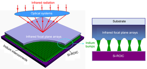
Figure 1
(Color online) Schematic diagram of focal plane array photovoltaic infrared detector.
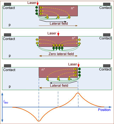
Figure 2
(Color online) The principle of a single n+-on-p pixel LBIC testing. Reprinted with permission from ref.
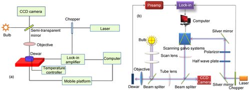
Figure 3
(Color online) Two different structure frames of laser beam induced current (LBIC) test system. (a) Scanning is performed by changing position of sample under control of a two-dimensional mobile platform; (b) scanning is performed by changing the direction of the laser beam under control of a scanning galvo system.
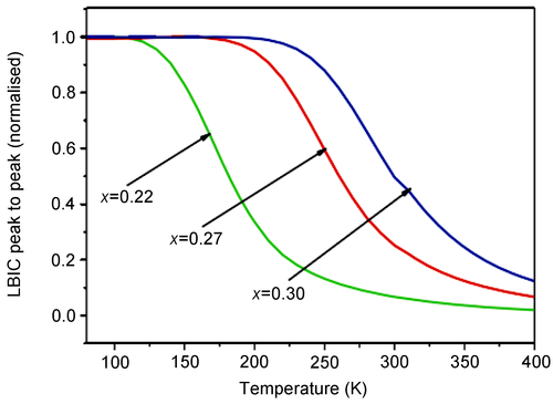
Figure 4
(Color online) Simulated LBIC peak-to-peak magnitudes as a function of temperature in Hg1-
Figure 5
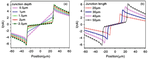
(Color online) (a) LBIC profiles with different depths of Hg0.69Cd0.31Te p-n junction and (b) LBIC profiles with different lengths of Hg0.69Cd0.31Te p-n junction. Reprinted with permission from ref.
Figure 6
(Color online) (a) The standard diffusion length (
Figure 7
(Color online) The LBIC test for characteristic diffusion length (
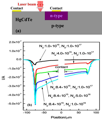
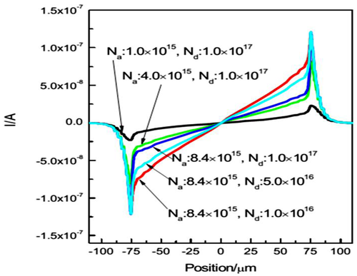
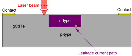
Figure 8
(Color online) The model structure of the p-n junction with localized junction leakage path along the horizontal portion of the junction.
Figure 9
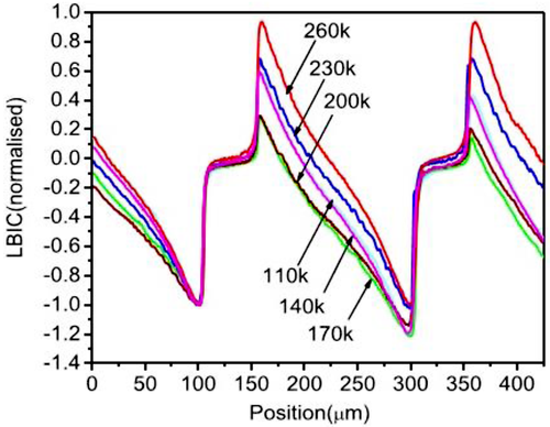
(Color online) The LBIC measurements are taken at a range of temperatures from 110 K to 260 K. Reprinted with permission from ref.
Figure 10
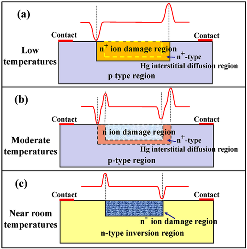
(Color online) Proposed p-n junction transformation models (a) at low temperature where the typical n+-on-p junction is formed, (b) at moderate temperature where the n-n+-on-p junction is formed, and (c) at near room temperature where the n--on-n junction are formed. Reprinted with permission from ref.
Figure 11
(Color online) Temperature dependency of Hall coefficients. The
Figure 12
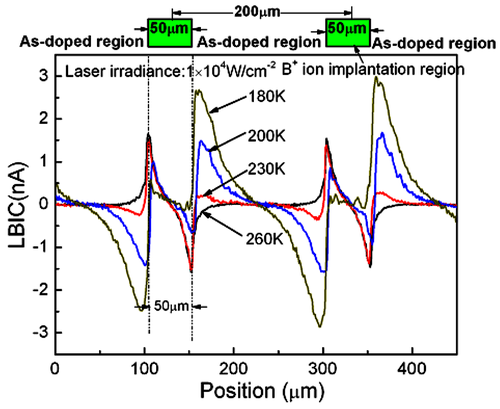
(Color online) Experimental results of temperature-dependent LBIC signal profiles with a laser power density of 1×10⁴ W/cm2. Reprinted with permission from ref.
Figure 13
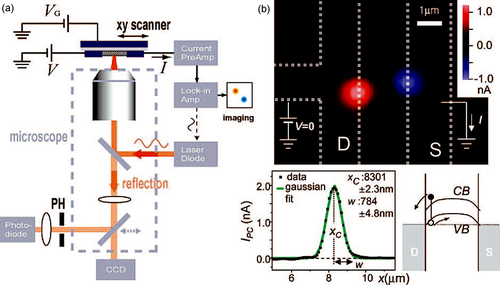
(Color online) (a) Schematic diagram of the SPCM setup. (b) SPCM image of a semiconducting CNT device D1. Left inset: Gaussian fit of one PC spot for determining the peak position and width. Right inset: physical mechanism of the contact PC generation. Reprinted with permission from ref.
Figure 14
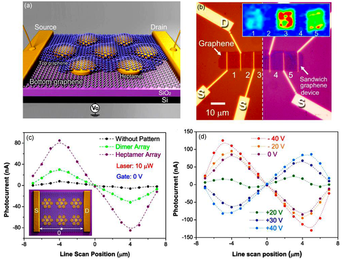
(Color online) Photocurrent characterization of antenna-graphene sandwich devices. (a) Schematic illustration of a single gold heptamer sandwiched between two monolayer graphene sheets.
Figure 15
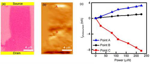
(Color online) (a) Optical image of a back-gated typical graphene field effect transistor. (b) LBIC mapping at room temperature with the laser wavelength of
Figure 16
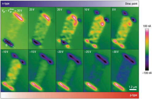
(Color online) Spatially resolved photocurrent maps at various transport regimes of a graphene device. The sequence of images displaying the n- to p-type transition, as the gate voltage is swept from 30 to
Figure 17
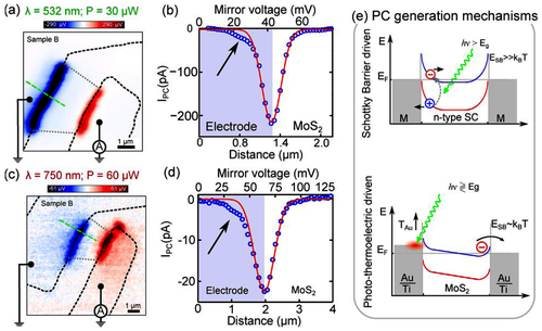
(Color online) Photovoltage map of a single layer MoS2 FET using an excitation wavelength of 532 nm (a) and 750 nm (c). (b), (d) Photocurrent profile across the line cut in panels a, b (open blue circles). The solid red line is a Gaussian fit of the data and the arrow points at the photocurrent tail generated when the laser spot is scanned over the electrode. (e) Schematic of the photoresponse mechanism in a device dominated by photothermoelectric effect. The conduction band is drawn in blue while the valence band is drawn in red. Reprinted with permission from ref.
Parameters |
Expression |
Abbt |
|
Kn,p |
(1015 cm-3) |
(1017 cm-3) |
Characteristic diffusion length |
Standard diffusion length |
L/Lp |
1.0 |
1.0 |
8.34 |
7.81 |
1.07 |
4.0 |
1.0 |
6.09 |
5.73 |
1.06 |
8.4 |
1.0 |
5.34 |
4.97 |
1.07 |
8.4 |
5.0 |
5.41 |
5.02 |
1.08 |
8.4 |
1.0 |
5.40 |
5.06 |
1.07 |


Copyright 2019 Science China Press Co., Ltd. 科学大众杂志社有限责任公司 版权所有
京ICP备18024590号-1

 Download PDF
